Browsing Advanced Materials for Micro- and Nano-Systems (AMMNS) by Title
Now showing items 12-31 of 122
-
Characterization of ZnO Nanorods Grown on GaN Using Aqueous Solution Method
(2005-01)Uniformly distributed ZnO nanorods with diameter 70-100 nm and 1-2μm long have been successfully grown at low temperatures on GaN by using the inexpensive aqueous solution method. The formation of the ZnO nanorods and the ... -
Charge Storage Effect in a Trilayer Structure Comprising Germanium Nanocrystals
(2002-01)A metal-insulator-semiconductor (MIS) device with a trilayer insulator structure consisting of sputtered SiO₂ (~50nm)/evaporated pure germanium (Ge) layer (2.4nm)/rapid thermal oxide (~5nm) was fabricated on a p-type ... -
Charge storage in nanocrystal systems: Role of defects?
(2004-01)Wet thermal oxidations of polycrystalline Si₀.₅₄Ge₀.₄₆ films at 600°C for 30 and 50 min were carried out. A stable mixed oxide was obtained for films that were oxidized for 50 min. ... -
Charge Storage Mechanism and Size Control of Germanium Nanocrystals in a Tri-layer Insulator Structure of a MIS Memory Device
(2003-01)A method of synthesizing and controlling the size of germanium nanocrystals is developed. A tri-layer metal-insulator-semiconductor (MIS) memory device structure comprising of a thin (~5nm) silicon dioxide (SiO₂) ... -
Computation and Simulation of the Effect of Microstructures on Material Properties
(2002-01)Methods for and computed results of including the physics and spatial attributes of microstructures are presented for a number of materials applications in devices. The research in our group includes applications of ... -
Computation and Simulation of the Effect of Microstructures on Material Properties
(2003-01)Many material properties depend on specific details of microstructure and both optimal material performance and material reliability often correlate directly to microstructure. In nano- and micro-systems, the material's ... -
A Constitutive Model for the Mechanical Behavior of Single Crystal Silicon at Elevated Temperature
(2002-01)Silicon in single crystal form has been the material of choice for the first demonstration of the MIT microengine project. However, because it has a relatively low melting temperature, silicon is not an ideal material for ... -
A continuum theory of amorphous solids undergoing large deformations, with application to polymeric glasses
(2003-01)This paper summarizes a recently developed continuum theory for the elastic-viscoplastic deformation of amorphous solids such as polymeric and metallic glasses. Introducing an internal-state variable that represents the ... -
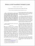
Defects in Self Assembled Colloidal Crystals
(2005-01)Colloidal self assembly is an efficient method for making 3-D ordered nanostructures suitable for materials such as photonic crystals and macroscopic solids for catalysis and sensor applications. Colloidal crystals grown ... -
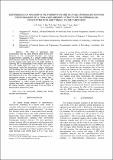
Dependence of nanocrystal formation and charge storage/retention performance of a tri-layer memory structure on germanium concentration and tunnel oxide thickness
(2004-01)The effect of germanium (Ge) concentration and the rapid thermal oxide (RTO) layer thickness on the nanocrystal formation and charge storage/retention capability of a trilayer metal-insulator-semiconductor device was ... -
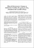
Effect of Microstructure Changes on Mechanical Properties of La₆₆Al₁₄(Cu, Ni)₂₀ Amorphous and Crystalline Alloys
(2004-01)The microstructure, and phase selections of La₆₆Al₁₄(Cu, Ni)₂₀ alloy were studied by Bridgman solidifications, and composite materials of dendrites in amorphous matrix or micro- ... -
Effect of Oxygen on Ni-Silicided FUSI Metal Gate
(2006-01)Continual evolution of the CMOS technology requires thinner gate dielectric to maintain high performance. However, when moving into the sub-65 nm CMOS generation, the traditional poly-Si gate approach cannot effectively ... -
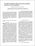
The Effect of Periodic Silane Burst on the Properties of GaN on Si (111) Substrates
(2005-01)The periodic silane burst technique was employed during metalorganic chemical vapor deposition of epitaxial GaN on AlN buffer layers grown on Si (111). Periodic silicon delta doping during growth of both the AlN and GaN ... -
Effect of Pt on agglomeration and Ge out-diffusion in Ni(Pt) germanosilicide
(2004-01)The effect of Ni and Ni(Pt) alloy with ~5 and 10 at. % Pt on the agglomeration and Ge out-diffusion in Nickel germanosilicide formed on Si₀.₇₅Ge₀.₂₅(100) has been studied. A ... -
Effect of Wafer Bow and Etch Patterns in Direct Wafer Bonding
(2003-01)Direct wafer bonding has been identified as an en-abling technology for microelectromechanical systems (MEMS). As the complexity of devices increase and the bonding of multiple patterned wafers is required, there is a need ... -
Effects of Applied Loads, Effective Contact Area and Surface Roughness on the Dicing Yield of 3D Cu Bonded Interconnects
(2006-01)Bonded copper interconnects were created using thermo-compression bonding and the dicing yield was used as an indication of the bond quality. SEM images indicated that the Cu was plastically deformed. Our experimental and ... -
Effects of Platinum on NiPtSiGe/n-SiGe and NiPtSi/n-Si Schottky Contacts
(2005-01)Solid phase reaction of NiPt/Si and NiPt/SiGe is one of the key issues for silicide (germanosilicide) technology. Especially, the NiPtSiGe, in which four elements are involved, is a very complex system. As a result, a ... -
Electrochemical Behavior and Li Diffusion Study of LiCoO₂ Thin Film Electrodes Prepared by PLD
(2007-01)Preferred c-axis oriented LiCoO₂ thin films were prepared on the SiO₂/Si (SOS) substrates by pulsed laser deposition (PLD). Thin film electrodes without carbon and binder are ideal samples to study the electrochemical ... -
Enhancement in Indium Incorporation for InGaN Grown on InN Intermediate Layer
(2006-01)InN has been grown on GaN with a thin intermediate layer of InGaN by metalorganic chemical vapor deposition (MOCVD) to further enhance indium incorporation in subsequent InGaN layer. Trimethylindium (TMI) and ammonia (NH₃) ... -
Evolution of AlN buffer layers on Silicon and the effect on the property of the expitaxial GaN film
(2003-01)The morphology evolution of high-temperature grown AlN nucleation layers on (111) silicon has been studied using atomic force microscopy (AFM). The structure and morphology of subsequently grown GaN film were characterized ...