
Search
Now showing items 1-9 of 9
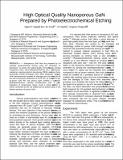
High Optical Quality Nanoporous GaN Prepared by Photoelectrochemical Etching
(2005-01)
Nanoporous GaN films are prepared by UV assisted electrochemical etching using HF solution as an electrolyte. To assess the optical quality and morphology of these nanoporous films, micro-photoluminescence (PL), micro-Raman ...
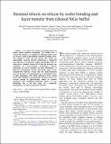
Strained Silicon on Silicon by Wafer Bonding and Layer Transfer from Relaxed SiGe Buffer
(2005-01)
We report the creation of strained silicon on silicon (SSOS) substrate technology. The method uses a relaxed SiGe buffer as a template for inducing tensile strain in a Si layer, which is then bonded to another Si handle ...
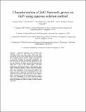
Characterization of ZnO Nanorods Grown on GaN Using Aqueous Solution Method
(2005-01)
Uniformly distributed ZnO nanorods with diameter 70-100 nm and 1-2μm long have been successfully grown at low temperatures on GaN by using the inexpensive aqueous solution method. The formation of the ZnO nanorods and the ...
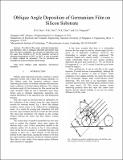
Oblique Angle Deposition of Germanium Film on Silicon Substrate
(2005-01)
The effect of flux angle, substrate temperature and deposition rate on obliquely deposited germanium (Ge) films has been investigated. By carrying out deposition with the vapor flux inclined at 87° to the substrate normal ...
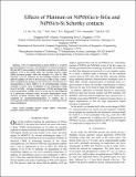
Effects of Platinum on NiPtSiGe/n-SiGe and NiPtSi/n-Si Schottky Contacts
(2005-01)
Solid phase reaction of NiPt/Si and NiPt/SiGe is one of the key issues for silicide (germanosilicide) technology. Especially, the NiPtSiGe, in which four elements are involved, is a very complex system. As a result, a ...
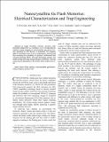
Nanocrystalline Ge Flash Memories: Electrical Characterization and Trap Engineering
(2005-01)
Conventional floating gate non-volatile memories (NVMs) present critical issues for device scalability beyond the sub-90 nm node, such as gate length and tunnel oxide thickness reduction. Nanocrystalline germanium (nc-Ge) ...
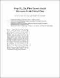
Poly-Si₁â‚‹xGex Film Growth for Ni Germanosilicided Metal Gate
(2005-01)
Scaling down of the CMOS technology requires thinner gate dielectric to maintain high performance. However, due to the depletion of poly-Si gate, it is difficult to reduce the gate thickness further especially for sub-65 ...
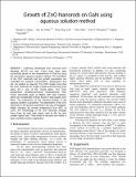
Growth of ZnO Nanorods on GaN Using Aqueous Solution Method
(2005-01)
Uniformly distributed ZnO nanorods with
diameter 80-120 nm and 1-2µm long have been
successfully grown at low temperatures on GaN by using the inexpensive aqueous solution method. The formation of the ZnO nanorods and ...
High Indium Concentration InGaN/GaN Grown on Sapphire Substrate by MOCVD
(2005-01)
The InGaN system provides the opportunity to fabricate light emitting devices over the whole visible and ultraviolet spectrum due to band-gap energies E[subscript g] varying between 3.42 eV for GaN and 1.89 eV for InN. ...