
Search
Now showing items 1-5 of 5
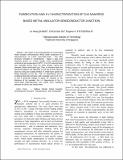
Fabrication and I-V Characterization of ZnO Nanorod Based Metal-Insulator-Semiconductor Junction
(2006-01)
We report on the characteristics of a ZnO based metal insulator semiconductor (MIS) diode comprised of a heterostructure of n-ZnO nanorods/n-GaN. The MIS structure consisted of unintentional - doped n type ZnO nanorods ...
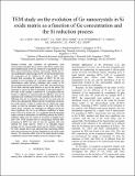
TEM Study on the Evolution of Ge Nanocrystals in Si Oxide Matrix as a Function of Ge Concentration and the Si Reduction Process
(2006-01)
Growth and evolution of germanium (Ge) nanocrystals embedded into a silicon oxide (SiO₂) system have been studied based on the Ge content of co-sputtered Ge-SiO₂ films using transmission electron microscopy (TEM) and X-ray ...

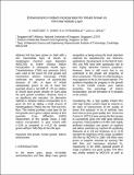
Effect of Oxygen on Ni-Silicided FUSI Metal Gate
(2006-01)
Continual evolution of the CMOS technology requires thinner gate dielectric to maintain high performance. However, when moving into the sub-65 nm CMOS generation, the traditional poly-Si gate approach cannot effectively ...
Enhancement in Indium Incorporation for InGaN Grown on InN Intermediate Layer
(2006-01)
InN has been grown on GaN with a thin intermediate layer of InGaN by metalorganic chemical vapor deposition (MOCVD) to further enhance indium incorporation in subsequent InGaN layer. Trimethylindium (TMI) and ammonia (NH₃) ...
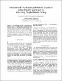
Fabrication of Two-Dimensional Photonic Crystals in AlGaInP/GaInP Membranes by Inductively Coupled Plasma Etching
(2006-01)
The fabrication process of two-dimensional photonic crystals in an AlGaInP/GaInP multi-quantum-well membrane structure is developed. The process includes high resolution electron-beam lithography, pattern transfer into ...