| dc.contributor.author | Musso, Tiziana | |
| dc.contributor.author | Kumar, Priyank V. | |
| dc.contributor.author | Foster, Adam S. | |
| dc.contributor.author | Grossman, Jeffrey C. | |
| dc.date.accessioned | 2016-03-30T17:22:26Z | |
| dc.date.available | 2016-03-30T17:22:26Z | |
| dc.date.issued | 2014-10 | |
| dc.date.submitted | 2014-08 | |
| dc.identifier.issn | 1936-0851 | |
| dc.identifier.issn | 1936-086X | |
| dc.identifier.uri | http://hdl.handle.net/1721.1/101938 | |
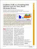
| dc.description.abstract | The excellent physical and semiconducting properties of transition metal dichalcogenide (TMDC) monolayers make them promising materials for many applications. The TMDC monolayer MoS[subscript 2] has gained significant attention as a channel material for next-generation transistors. However, while n-type single-layer MoS2 devices can be made with relative ease, fabrication of p-type transistors remains a challenge as the Fermi-level of elemental metals used as contacts are pinned close to the conduction band leading to large p-type Schottky barrier heights (SBH). Here, we propose the utilization of graphene oxide (GO) as an efficient hole injection layer for single-layer MoS[subscript 2]-based electronic and optoelectronic devices. Using first-principles computations, we demonstrate that GO forms a p-type contact with monolayer MoS[subscript 2], and that the p-type SBH can be made smaller by increasing the oxygen concentration and the fraction of epoxy functional groups in GO. Our analysis shows that this is possible due to the high work function of GO and the relatively weak Fermi-level pinning at the MoS[subscript 2]/GO interfaces compared to traditional MoS[subscript 2]/metal systems (common metals are Ag, Al, Au, Ir, Pd, Pt). The combination of easy-to-fabricate and inexpensive GO with MoS[subscript 2] could be promising for the development of hybrid all-2D p-type electronic and optoelectronic devices on flexible substrates. | en_US |
| dc.description.sponsorship | Eni S.p.A. (Firm) (Eni-MIT Alliance Solar Frontiers Program) | en_US |
| dc.language.iso | en_US | |
| dc.publisher | American Chemical Society (ACS) | en_US |
| dc.relation.isversionof | http://dx.doi.org/10.1021/nn504507u | en_US |
| dc.rights | Article is made available in accordance with the publisher's policy and may be subject to US copyright law. Please refer to the publisher's site for terms of use. | en_US |
| dc.source | MIT web domain | en_US |
| dc.title | Graphene Oxide as a Promising Hole Injection Layer for MoS[subscript 2]-based Electronic Devices | en_US |
| dc.type | Article | en_US |
| dc.identifier.citation | Musso, Tiziana, Priyank V. Kumar, Adam S. Foster, and Jeffrey C. Grossman. “Graphene Oxide as a Promising Hole Injection Layer for MoS[subscript 2]-Based Electronic Devices.” ACS Nano 8, no. 11 (November 25, 2014): 11432–11439. | en_US |
| dc.contributor.department | Massachusetts Institute of Technology. Department of Materials Science and Engineering | en_US |
| dc.contributor.mitauthor | Kumar, Priyank V. | en_US |
| dc.contributor.mitauthor | Grossman, Jeffrey C. | en_US |
| dc.relation.journal | ACS Nano | en_US |
| dc.eprint.version | Author's final manuscript | en_US |
| dc.type.uri | http://purl.org/eprint/type/JournalArticle | en_US |
| eprint.status | http://purl.org/eprint/status/PeerReviewed | en_US |
| dspace.orderedauthors | Musso, Tiziana; Kumar, Priyank V.; Foster, Adam S.; Grossman, Jeffrey C. | en_US |
| dc.identifier.orcid | https://orcid.org/0000-0003-1281-2359 | |
| mit.license | PUBLISHER_POLICY | en_US |
