Dislocations behavior in highly mismatched III-Sb growth and their impact on the fabrication of top-down n + InAs/p + GaSb nanowire tunneling devices
Author(s)
El Kazzi, S; Alian, A; Hsu, B; Favia, P; Merckling, C; Lu, W; del Alamo, JA; Collaert, N; ... Show more Show less
DownloadPublished version (2.129Mb)
Terms of use
Metadata
Show full item recordAbstract
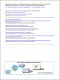
© 2018 Author(s). We study in this work the growth and fabrication of top-down highly doped n + InAs(Si)/p + GaSb(Si) Esaki tunneling diodes on (001) GaAs substrates. A careful investigation on the highly mismatched GaSb/GaAs growth is first conducted by means of Reflection High-Energy Electron Diffraction (RHEED), Atomic Force Microscopy (AFM), and X-Ray Diffraction (XRD) analyses. These results are expected to pave the way to methods for III-Sb buffer layer's integration with low threading dislocation (TD) densities. A comparison between AFM, XRD, defect revealing by chemical etching and transmission electron microscopy (TEM) is then presented to calculate the precise TD density and its influence on the device structure. In the last part, we report on first operating sub-30 nm III-V vertical NW tunneling devices on (001) commercial GaAs substrates.
Date issued
2018Department
Massachusetts Institute of Technology. Microsystems Technology LaboratoriesJournal
Journal of Applied Physics
Publisher
AIP Publishing