Browsing Advanced Materials for Micro- and Nano-Systems (AMMNS) by Title
Now showing items 75-94 of 122
-
Nanocomposite Thin Films for both Mechanical and Functional Applications
(2004-01)The design methodology and realization of nanocomposite films aiming for mechanical (superhardness, toughness) and functional (optical, microelectronic) properties were discussed in this paper. Superhard TiCrCN and ... -
Nanocrystalline Ge Flash Memories: Electrical Characterization and Trap Engineering
(2005-01)Conventional floating gate non-volatile memories (NVMs) present critical issues for device scalability beyond the sub-90 nm node, such as gate length and tunnel oxide thickness reduction. Nanocrystalline germanium (nc-Ge) ... -
Native Point Defects in yttria as a High-Dielectric-Constant Gate Oxide Material: A First-Principles Study
(2006-01)Yttria (Y₂O₃) has become a promising gate oxide material to replace silicon dioxide in metal-oxide-semiconductor (MOS) devices. The characterization of native point defect in Y₂O₃ is essential to understand the behavior ... -
Novel CMOS-Compatible Optical Platform
(2003-01)A research synopsis is presented summarizing work with integration of Ge and III-V semiconductors and optical devices with Si. III-V GaAs/AlGaAs quantum well lasers and GaAs/AlGaAs optical circuit structures have been ... -
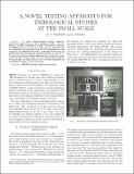
A Novel Testing Apparatus for Tribological Studies at the Small Scale
(2002-01)A novel flexure-based biaxial compression/shear apparatus has been designed, built, and utilized to conduct tribological studies of interfaces relevant to MEMS. Aspects of our new apparatus are detailed and its capabilities ... -
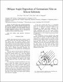
Oblique Angle Deposition of Germanium Film on Silicon Substrate
(2005-01)The effect of flux angle, substrate temperature and deposition rate on obliquely deposited germanium (Ge) films has been investigated. By carrying out deposition with the vapor flux inclined at 87° to the substrate normal ... -
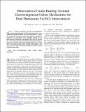
Observation of Joule Heating-Assisted Electromigration Failure Mechanisms for Dual Damascene Cu/SiO₂ Interconnects
(2003-01)Failure mechanisms observed in electromigration (EM) stressed dual damascene Cu/SiO₂ interconnects trees were studied and simulated. Failure sites with ‘melt patch’ or ‘crater’ are common for test structures in the top ... -
Optically pumped InxGa₁â‚‹xN/InyGa₁â‚‹yN multiple quantum well vertical cavity surface emitting laser operating at room temperature.
(2004-01)Room temperature vertical cavity lasing at the wavelength of 433nm has been successfully realized in InxGa₁â‚‹xN/InyGa₁â‚‹yN multiple quantum well without Bragg mirrors under photo-excitation. At high excitation intensity, ... -
Ordering Control of Self-Assembled Colloidal Crystals
(2007-01)Colloidal crystals are 3D nanostructures formed by self assembly of nanoparticles in suspension. The interaction forces between the colloid particles are expected to affect the ordering and the defect density in the resultant ... -
Orientation of MgO thin films on Si(001) prepared by pulsed laser deposition
(2003-01)Pulsed laser deposition method was employed to grow MgO thin films with preferred orientation on bare Si(100) and SiO₂/Si(100) substrates. The orientation of MgO thin films was systematically investigated by varying ... -
PALM: Predicting Internet Network Distances Using Peer-to-Peer Measurements
(2004-01)Landmark-based architecture has been commonly adopted in the networking community as a mechanism to measure and characterize a host's location on the Internet. In most existing landmark based approaches, end hosts use the ... -
Photonic Crystals: Numerical Predictions of Manufacturable Dielectric Composite Architectures
(2004-01)Photonic properties depend on both dielectric contrast in a microscopic composite and the arrangement of the microstructural components. No theory exists for direct prediction of photonic properties, and so progress relies ... -
Plastic Relaxation In Single InᵡGa₁â‚‹ᵡN/GaN Epilayers Grown On Sapphire
(2004-01)Plastic relaxation was observed in InᵡGa₁â‚‹ᵡN/GaN epilayers grown on c-plane sapphire substrates. The relaxation obeys the universal hyperbolic relation between the strain and the reciprocal of the layer ... -
Poly-Si₁â‚‹xGex Film Growth for Ni Germanosilicided Metal Gate
(2005-01)Scaling down of the CMOS technology requires thinner gate dielectric to maintain high performance. However, due to the depletion of poly-Si gate, it is difficult to reduce the gate thickness further especially for sub-65 ... -
Preliminary Characterisation of Low-Temperature Bonded Copper Interconnects for 3-D Integrated Circuits
(2005-01)Three dimensional (3-D) integrated circuits can be fabricated by bonding previously processed device layers using metal-metal bonds that also serve as layer-to-layer interconnects. Bonded copper interconnects test structures ... -
Process development of silicon-silicon carbide hybrid structures for micro-engines (January 2002)
(2002-01)MEMS-based gas turbine engines are currently under development at MIT for use as a button-sized portable power generator or micro-aircraft propulsion sources. Power densities expected for the micro-engines require very ... -
Processing, Structure, Properties, and Reliability of Metals for Microsystems
(2002-01)Research on the processing, structure, properties and reliability of metal films and metallic microdevice elements is reviewed. Recent research has demonstrated that inelastic deformation mechanisms of metallic films and ... -
Progress in Developing and Extending RM³ Heterogeneous Integration Technologies
(2003-01)This paper describes recent progress in a continuing program to develop and apply RM³ (recess mounting with monolithic metallization) technologies for heterogeneous integration. Particular emphasis is placed on the APB ... -
Reliability of Multi-Terminal Copper Dual-Damascene Interconnect Trees
(2003-01)Electromigration tests on different Cu dual-damascene interconnect tree structures consisting of various numbers of straight via-to-via lines connected at the common middle terminal have been carried out. Like Al-based ... -
Research on Polycrystalline Films for Micro- and Nano-Systems
(2003-01)Polycrystalline films are used in a wide array of micro- and nano-scale devices, for electronic, mechanical, magnetic, photonic and chemical functions. Increasingly, the properties, performance, and reliability of films ...