| dc.contributor.author | Makaram, Prashanth | |
| dc.contributor.author | Joh, Jungwoo | |
| dc.contributor.author | del Alamo, Jesus A. | |
| dc.contributor.author | Palacios, Tomas | |
| dc.contributor.author | Thompson, Carl V. | |
| dc.date.accessioned | 2012-08-27T17:19:52Z | |
| dc.date.available | 2012-08-27T17:19:52Z | |
| dc.date.issued | 2010-06 | |
| dc.date.submitted | 2010-05 | |
| dc.identifier.issn | 0003-6951 | |
| dc.identifier.issn | 1077-3118 | |
| dc.identifier.uri | http://hdl.handle.net/1721.1/72346 | |
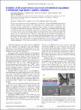
| dc.description.abstract | We have investigated the surface morphology of electrically stressed AlGaN/GaN high electron mobility transistors using atomic force microscopy and scanning electron microscopy after removing the gate metallization by chemical etching. Changes in surface morphology were correlated with degradation in electrical characteristics. Linear grooves formed along the gate edges in the GaN cap layer for all electrically stressed devices. Beyond a critical voltage that corresponds to a sharp increase in the gate leakage current, pits formed on the surface at the gate edges. The density and size of the pits increase with stress voltage and time and correlate with degradation in the drain current and current collapse. We believe that high mechanical stress in the AlGaN layer due to high-voltage stressing is relieved by the formation of these defects which act as paths for gate leakage current and result in electron trapping and degradation in the transport properties of the channel underneath. | en_US |
| dc.description.sponsorship | United States. Office of Naval Research (Grant number N00014-08-1-0655) | en_US |
| dc.description.sponsorship | United States. Army Research Laboratory (Contract Number W911QX-05-C-0087) | en_US |
| dc.language.iso | en_US | |
| dc.publisher | American Institute of Physics (AIP) | en_US |
| dc.relation.isversionof | http://dx.doi.org/10.1063/1.3446869 | en_US |
| dc.rights | Article is made available in accordance with the publisher's policy and may be subject to US copyright law. Please refer to the publisher's site for terms of use. | en_US |
| dc.source | MIT web domain | en_US |
| dc.title | Evolution of structural defects associated with electrical degradation in AlGaN/GaN high electron mobility transistors | en_US |
| dc.type | Article | en_US |
| dc.identifier.citation | Makaram, Prashanth et al. “Evolution of Structural Defects Associated with Electrical Degradation in AlGaN/GaN High Electron Mobility Transistors.” Applied Physics Letters 96.23 (2010): 233509. © 2010 American Institute of Physics | en_US |
| dc.contributor.department | MIT Materials Research Laboratory | en_US |
| dc.contributor.department | Massachusetts Institute of Technology. Department of Electrical Engineering and Computer Science | en_US |
| dc.contributor.department | Massachusetts Institute of Technology. Department of Materials Science and Engineering | en_US |
| dc.contributor.department | Massachusetts Institute of Technology. Microsystems Technology Laboratories | en_US |
| dc.contributor.approver | del Alamo, Jesus A. | |
| dc.contributor.mitauthor | Makaram, Prashanth | |
| dc.contributor.mitauthor | Joh, Jungwoo | |
| dc.contributor.mitauthor | del Alamo, Jesus A. | |
| dc.contributor.mitauthor | Palacios, Tomas | |
| dc.contributor.mitauthor | Thompson, Carl V. | |
| dc.relation.journal | Applied Physics Letters | en_US |
| dc.eprint.version | Final published version | en_US |
| dc.type.uri | http://purl.org/eprint/type/JournalArticle | en_US |
| eprint.status | http://purl.org/eprint/status/PeerReviewed | en_US |
| dspace.orderedauthors | Makaram, Prashanth; Joh, Jungwoo; del Alamo, Jesús A.; Palacios, Tomás; Thompson, Carl V. | en |
| dc.identifier.orcid | https://orcid.org/0000-0002-0121-8285 | |
| dc.identifier.orcid | https://orcid.org/0000-0002-2190-563X | |
| mit.license | PUBLISHER_POLICY | en_US |
| mit.metadata.status | Complete | |
