Browsing Advanced Materials for Micro- and Nano-Systems (AMMNS) by Title
Now showing items 61-80 of 122
-
Laser Fabrication by Using Photonic Crystal
(2003-01)This paper involves the calculation for composition of different layer used in laser structure and the simulation of cavity, formed by creating air columns in the InGaAsP medium, for square lattice. The aim of this project ... -
Length Effects on the Reliability of Dual-Damascene Cu Interconnects
(2002-01)The effects of interconnect length on the reliability of dual-damascene Cu metallization have been investigated. As in Al-based interconnects, the lifetimes of Cu lines increase with decreasing length. However, unlike ... -
Magnetically-Assisted Statistical Assembly - a new heterogeneous integration technique
(2002-01)This paper presents a new technique for the monolithic heterogeneous integration of compound semiconductor devices with silicon integrated circuits, and establishes the theoretical foundation for a key element of the ... -
Mechanical Characterization of the Heat Affected Zone of Gold Wirebonds Using Nanoindentation
(2002-01)With increasing miniaturization in microelectronics the wirebonds used in IC packages are witnessing a thrust towards fine pitch wirebonding. To have a precise control over loop height of the wirebond for fine pitch ... -
Mechanical Properties of Bulk Metallic Glasses and Composites
(2004-01)We have studied the mechanical properties of monolithic bulk metallic glasses and composite in the La based alloys. La₈₆₋yAl₁₄(Cu, Ni)y (y=24 to 32) alloy systems was used to cast the ... -
Mechanical properties of La-based bulk amorphous alloy and composites
(2003-01)Influence of different microstructure of La-based fully amorphous samples and its composites on the impact fracture energy were investigated and discussed. Results showed improvement in fracture energy of glassy metals ... -
MEMS Materials and Processes: a research overview
(2003-01)An overview is provided of materials and processes research currently being conducted in support of MEMS device design at MIT. Underpinning research is being conducted in five areas: room temperature strength characterization, ... -
Metallic Cluster Coalescence: Molecular Dynamics Simulations of Boundary Formation
(2003-01)During the evaporative deposition of polycrystalline thin films, the development of a tensile stress at small film thicknesses is associated with island coalescence. Several continuum models exist to describe the magnitude ... -
Metastable Intermediate in LixMnO₂ Layered to Spinel Phase Transition
(2002-01)Ab Initio calculations suggest that partially lithiated layered LixMnO₂ transforms to spinel in a two-stage process. In the first stage, a significant fraction of the Mn and Li ions rapidly occupy tetrahedral sites, forming ... -
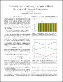
Methods for Calculating the Optical Band Structure of Photonic Composites
(2002-01)Lately, there has been an increasing interest in studying the propagation of electromagnetic waves in periodic dielectric structures (photonic crystals). Like the electron propagation in semiconductors, these structures ... -
Micro Raman Spectroscopy of Annealed Erbium Implanted GaN
(2004-01)Wurtzite GaN epilayers grown by metal organic chemical vapor deposition on sapphire substrates were subsequently ion implanted with Er to a dose of 5×10¹⁵ cm⁻². The implanted samples were annealed in nitrogen atmosphere ... -
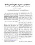
Monitoring Defect Formation in Colloidal Self Assembly using Photonic Bandgap Variations
(2006-01)Defect control in colloidal crystals is essential for these nanostructures to be effective as photonic bandgap (PBG) materials. We have used in-situ monitoring of the PBG of a colloidal crystal to study the structural ... -
Mortality Dependence of Cu Dual Damascene Interconnects on Adjacent Segments
(2004-01)Electromigration experiments have been carried out on straight interconnects that have single vias at each end, and are divided into two segments by a via in the center ("dotted-I" structures). For dotted-i structures in ... -
MOSFET Channel Engineering using Strained Si, SiGe, and Ge Channels
(2003-01)Biaxial tensile strained Si grown on SiGe virtual substrates will be incorporated into future generations of CMOS technology due to the lack of performance increase with scaling. Compressively strained Ge-rich alloys with ... -
Nanocomposite Thin Films for both Mechanical and Functional Applications
(2004-01)The design methodology and realization of nanocomposite films aiming for mechanical (superhardness, toughness) and functional (optical, microelectronic) properties were discussed in this paper. Superhard TiCrCN and ... -
Nanocrystalline Ge Flash Memories: Electrical Characterization and Trap Engineering
(2005-01)Conventional floating gate non-volatile memories (NVMs) present critical issues for device scalability beyond the sub-90 nm node, such as gate length and tunnel oxide thickness reduction. Nanocrystalline germanium (nc-Ge) ... -
Native Point Defects in yttria as a High-Dielectric-Constant Gate Oxide Material: A First-Principles Study
(2006-01)Yttria (Y₂O₃) has become a promising gate oxide material to replace silicon dioxide in metal-oxide-semiconductor (MOS) devices. The characterization of native point defect in Y₂O₃ is essential to understand the behavior ... -
Novel CMOS-Compatible Optical Platform
(2003-01)A research synopsis is presented summarizing work with integration of Ge and III-V semiconductors and optical devices with Si. III-V GaAs/AlGaAs quantum well lasers and GaAs/AlGaAs optical circuit structures have been ... -
A Novel Testing Apparatus for Tribological Studies at the Small Scale
(2002-01)A novel flexure-based biaxial compression/shear apparatus has been designed, built, and utilized to conduct tribological studies of interfaces relevant to MEMS. Aspects of our new apparatus are detailed and its capabilities ... -
Oblique Angle Deposition of Germanium Film on Silicon Substrate
(2005-01)The effect of flux angle, substrate temperature and deposition rate on obliquely deposited germanium (Ge) films has been investigated. By carrying out deposition with the vapor flux inclined at 87° to the substrate normal ...